
High-purity Gallium
High-purity Gallium
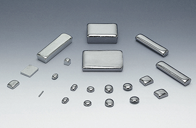
Gallium is an essential metal in the manufacture of semiconductors. It is widely used in LEDs, LDs, GaAs and GaN substrates, dopants, etc. Gallium is also expected to be used as a next-generation material for power semiconductor devices and is attracting attention as an important rare metal that supports advanced technologies. Contact Nichia through its website for customization of purities, weights, and shapes, and other specifications.
| Product Name | Gallium Metal |
|---|---|
| Chemical Formula | Ga |
| CAS No. | 7440-55-3 |
| Melting Point | 29.78℃ |
| Purity | 6N (99.9999%) 7N (99.99999%) |
| Weight/Piece | 1g~2,500g |
| Shape | Shot, Ingot, Bottled |
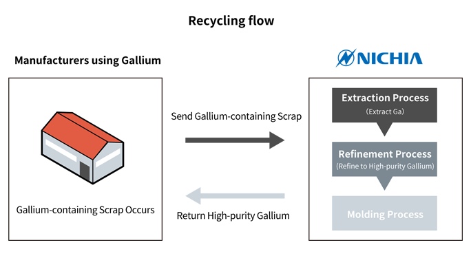
Gallium Recycling Business
In order to use limited resources efficiently, Nichia also operates a recycling business, extracting and refining gallium from gallium-containing scrap.
联系我们
For any questions or inquiries regarding Nichia's High-purity Gallium, use the contact form via the link below.
联系我们